
A Few-Dollar Wilkinson Divider: What Can It Really Do?
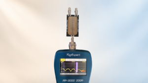
We wanted to receive satellite signals on our Fobos SDR receiver from two antennas at once. That calls for a divider (a combiner, in this direction). The simplest route was to buy a ready-made board from a marketplace for a few dollars. So we did. And then, instead of reaching for the soldering iron, we put it on the bench and measured it completely. Because before you put something into a signal path, it pays to know what exactly you are putting there.
The short version, for those reading on a phone:
- Matching: VSWR 1.5 class (worst -15.9 dB at 3.85 GHz). Not the 1.2 class one would like.
- Output-to-output isolation: better than 21 dB across the whole band. Respectable.
- Arm balance: 0.03 dB and 1.1 degrees. Excellent, better than expected.
- Excess loss: 0.4 dB at 0.5 GHz, but a full 2.7 dB at 4 GHz. The main drawback.
- Genuinely comfortable band: 0.5-2.5 GHz, not the claimed 0.5-4 GHz.
Let me walk you through how we measured it, why one methodological detail costs 2 dB in the result, and exactly where these drawbacks will bite you in real work.
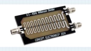
Our test subject: a multi-section 0.5-4 GHz Wilkinson divider. A meander of some ten quarter-wave sections with isolation resistors between the arms.
A Bit of Theory. Why a Wilkinson at All.
Let’s start with why you cannot just solder a tee. For DC, wiring loads in parallel is an everyday thing – the only limit on how many you can hang there is the power supply. For high-frequency AC it is a good deal trickier. Two 50-ohm loads in parallel make 25 ohms. The input of such a “divider” has a VSWR of 2.0 before you even connect anything to it. But that is not even the main trouble. The main one is that there is zero isolation between the two outputs: everything that leaks out of one output (a receiver’s LO, reflections from an antenna, the signal of the neighboring transmitter) sails straight into the other. For an antenna stack this means a distorted pattern, for two receivers – mutual interference, for two transmitters – intermodulation.
A resistive divider (three resistors in a star) solves the matching problem, but at the cost of loss: instead of the theoretical 3 dB you lose 6, and the isolation between outputs is the same miserable 6 dB. Its only real advantage is a very wide operating bandwidth.
And here enters the circuit that Ernest Wilkinson published back in 1960. Two quarter-wave line sections of 70.7 ohms and one 100-ohm resistor between the outputs.
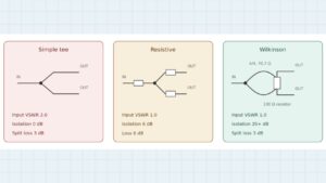
Fig. 1. Three ways to split a signal. The tee is cheap but neither matched nor isolating. The resistive one is matched but eats half the power. The Wilkinson gives you both.
How it works, on your fingers: the useful signal traveling from the input to the outputs arrives at both outputs in phase – the resistor sees equal potentials on both ends, no current flows through it, the resistor effectively does not exist. But a signal trying to sneak from one output into the other has two paths: a short one through the resistor and a long one around the half-ring of lines. These two paths produce out-of-phase waves that cancel each other, and the energy is neatly converted into heat in the resistor. The result is almost magic: all three ports matched, outputs isolated, and the loss is just the 3 dB of the split plus a small “tax” for non-ideality.
A single Wilkinson section holds decent parameters over roughly an octave. Our test subject claims an 8:1 band – 0.5 to 4 GHz. That is exactly why the board carries not one section but a cascade: a long meander of about ten quarter-wave links with a resistor in each. This is a classic multi-section Chebyshev divider, and this design detail will come in handy when we start reading the graphs.
How We Measured.
The measurements were done on a Siglent SVA1075X vector network analyzer with a full one-port SOLT calibration plus a transmission normalization, 751 points per 0.3-4.5 GHz sweep. The whole process is automated by a script: six connection configurations, from which the full 3×3 S-parameter matrix, a Touchstone file and a test report are assembled.
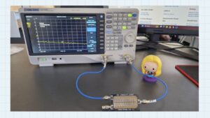
Fig. 2. The bench assembled. This shot was taken during a separate run, so the marker on the screen does not match the graphs below. Phoebe is keeping a close eye on the process.
And here is the first practical bonus for everyone who measures three-port devices with a two-port (let alone a one-path) instrument.
The methodological trap that costs 2 dB. The input match of a Wilkinson depends directly on what its outputs are terminated with. If one output hangs on the receiving port of the analyzer during the measurement, you are not measuring the board – you are measuring the board plus the imperfect match of that port, and you will “measure yourself” a result 1.5-2 dB worse than reality. We stepped on this rake, verified it and fixed the methodology: all reflections (S11, S22, S33) were taken with two quality 50-ohm loads on the free ports. The difference is exactly those 2 dB at the worst points. Remember this nuance – it deserves an article of its own, and it will get one.
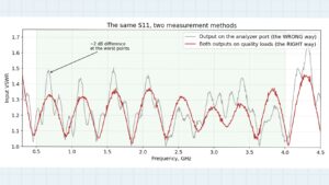
Fig. 3. The very same input of the board, two methods: the gray curve – one divider output terminated by the analyzer’s receiving port, the red one – both outputs on quality 50-ohm loads. The difference at the worst points is almost 2 dB.
Two Independent Checks.
The attentive reader will notice that we measured with another manufacturer’s instrument. So we checked part of the range a second time – with our RigExpert AA-3000 Zoom and the AntScope2 software. The setup is as clean as it gets: the board is bolted straight onto the analyzer through an adapter, no cable at all, both outputs terminated with 50 ohms. The calibration plane ends up right at the connector, and not a trace of cable ripple gets into the result.
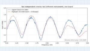
Fig. 4. Two instruments, one board. The hump and null frequencies agree to within the grid step, and the VSWR deviation at the humps is under 0.05.
Worst VSWR in the 1-3 GHz band: 1.386 according to the AA-3000 ZOOM and 1.368 according to the SVA1075X. The AA-3000 ZOOM found its VSWR minimum at 2320 MHz reading 1.03 – at that point we have 1.049 at 2316 MHz. In other words, the “VSWR 1.5 class” verdict is confirmed by two different instruments, two different calibration methods and two different measurement operators. Which is exactly what you want when publishing data about somebody else’s product.
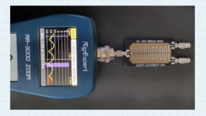
Fig. 5. The check with our own analyzer. VSWR minimum 1.03 at 2320 MHz.
What the Measurements Showed.
Matching. The input S11 plot shows a uniform “picket fence” of humps with a 0.44 GHz period. Anyone who read my article on reading a helix antenna’s VSWR plot will recognize a familiar picture: the ripple period is inversely proportional to the electrical length of the structure (Δf ≈ c/2L). Only, where the helix ripple was a parasitic reflection from the far end of the winding, here the equal-height, equally spaced humps are the normal Chebyshev signature of a multi-section transformer. And here we can cross-examine the board. An N-section Chebyshev transformer has exactly N reflection nulls in its passband and N-1 humps between them. Count them on the graph: ten dips (the outermost at 0.47 and 4.49 GHz, so the designed band is actually a bit wider than the label on the board) and nine humps. Count the resistors on the board: exactly ten. The math agrees with the soldering iron. The board behaves precisely as designed. The only question is WHAT it was designed for.
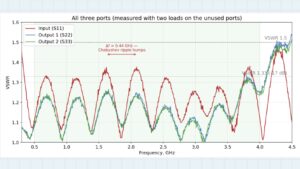
Fig. 6. VSWR of all three ports. Equally spaced humps with a 0.44 GHz period – the normal Chebyshev signature. The board sits confidently in the VSWR 1.5 class, but does not reach the 1.33 level (-17 dB) on the humps.
And it was designed for the VSWR 1.5 class. The worst points in the 0.5-4 GHz band:
- Input (S11): -15.9 dB at 3.85 GHz, VSWR 1.38. Humps worse than -17 dB: near 0.67, 1.6, 2.1 and 3.8-3.9 GHz.
- Output 1 (S22): -16.9 dB at 3.79 GHz.
- Output 2 (S33): -17.2 dB, formally the best of the three.
- Typical values between the humps: -18…-25 dB.
Isolation between outputs: no worse than 21 dB across the whole band, with a deep -42 dB null at 0.9 GHz. For such an enormously wide band – respectable.
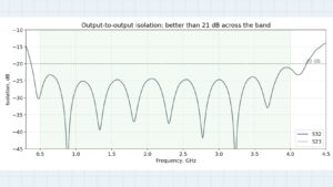
Fig. 7. Output-to-output isolation. Both directions (S23 and S32) fall right on top of each other – one more indirect proof of the measurement quality.
Arm balance: here the board was a pleasant surprise. Amplitude spread between the outputs – 0.03 dB, phase – 1.1 degrees across the whole band. The meander symmetry is executed well, and for tasks where the identity of the two channels is what matters (stacks, phased arrays) this is a strong argument.
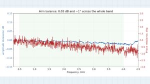
Fig. 8. Amplitude (blue curve, left scale) and phase (red, right scale) imbalance between the two outputs. Far more expensive devices would envy this balance.
Losses. And here comes the main “surprise”. Loss in one arm: 3.4 dB at 0.5 GHz (that is, only 0.4 dB of excess – excellent) and a whopping 5.7 dB at 4 GHz. The excess loss at the top edge of the band is 2.7 dB. The physics is simple and merciless: a 4 GHz signal has to run through all twenty-odd centimeters of the meander on an open microstrip made of cheap material, and along the way it gets eaten by the dielectric, the copper and radiation.
Fig. 9. Transmission into both arms. Up to 1.5 GHz the excess loss is 0.4-0.8 dB – the board works like a textbook. At 4 GHz it is already 2.7 dB on top of the theoretical 3: nearly half the power never reaches the outputs.
The Pros, (Honestly).
- An 8:1 band in a single board is genuinely convenient: one device covers everything from 0.5 GHz, including 23 cm, 13 cm and all the ISM bands up to 4 GHz… Wait, hold on – see the losses below.
- Excellent amplitude and phase balance. Better than you have any right to expect for this money.
- 21+ dB isolation across the whole band.
- The price. For this money you cannot buy even one decent flanged SMA connector (hi, Pasternack).
The Cons, and Where They Will Bite You.
- Losses in the upper half of the band (Fig. 9). This is con number one, and it is not cosmetic. Imagine combining the signals of two antennas at 3.5-4 GHz with this divider. Each signal brings along 2.7 dB of excess loss – nearly half the power turns into heat and radiation before it even reaches the output. In a receive chain this is +2.7 dB added to the noise figure of the whole system if the divider sits before the amplifier. The gain from the second antenna of a stack (+3 dB) gets almost entirely eaten. Below 1.5 GHz the situation is much better: excess losses of 0.4-0.8 dB, and the board works nearly by the book.
- Matching is VSWR 1.5 class, not 1.2 (Fig. 6). For receive tasks – mostly irrelevant. But in a measurement setup or a transmitter chain, VSWR 1.4-1.5 humps mean ripple in the passband response and extra measurement uncertainty. If you are building a bench for comparing antennas, keep in mind that the divider will add its own ±0.3-0.5 dB of waviness.
- The resistors and power handling. The 21 dB isolation works as long as the system is symmetric. But the moment you combine two transmitters and one of them drifts in phase, or one of the antennas falls off, the differential power goes off to heat those same tiny SMD resistors on the board. The manufacturer stays modestly silent about the power rating, and, looking at the resistor package size, we would not trust this board with more than a few hundred milliwatts of total asymmetry. For receiving – no questions. For power combining – only if you know exactly what you are doing.
- An open board. A microstrip without a shield not only radiates (part of those same losses) but also picks up. Put this board next to a switching power supply or a Wi-Fi router and it will faithfully mix the pickup into your signal path. Fine for the lab bench; for a field build, plan the shielding yourself.
- The band edges. The label says 0.5-4 GHz, and formally the board does work there. But the worst matching points sit right around 0.67 and 3.8 GHz, and the losses grow monotonically toward the upper edge. The genuinely comfortable zone of this board is roughly 0.5-2.5 GHz. Above that – only with a clear understanding of the trade-offs.
The Main Rule.
Just as a beautiful antenna VSWR says nothing about the radiation pattern, there is a rule here worth memorizing: the “0.5-4 GHz” print on the board guarantees only that the device formally functions in that band. How much it loses, how well it isolates and what it survives – the print does not say. Only measurements do.
The Bottom Line.
We have an honest workhorse for laughable money:
- for splitting a signal to two receivers, diversity reception, non-critical lab tasks up to 2.5 GHz – buy it and use it;
- for antenna stacks – yes, but do the loss budget at your frequency first;
- for combining transmitter power – carefully, and only at low levels;
- for precision measurement setups and the upper part of the band – look for something better.
For our original task – two satellite channels into a Fobos SDR around 1.5-2.3 GHz – the board is a fit (though one always wants better). Excess loss there is under a decibel, isolation is past 25 dB, the balance is exemplary. Had we wanted the same thing at 3.5-4 GHz, it would have been a different conversation.
The full Touchstone file (.s3p) with all six S-parameters is available for download. Use it, check it, argue with it – that is exactly why we are publishing it.
And one last thing. While I was running this board on the bench, in parallel I designed a Wilkinson divider of my own – a three-section one, optimized for the narrower 0.7-2.5 GHz range, which is exactly where 23 cm, 13 cm, GPS and ISM 2.4 live. The electromagnetic simulation shows numbers that made me raise an eyebrow, but simulation numbers are not a product yet. The boards are ordered and on their way to the very same measurement bench. Whatever the real measurements show is what we will publish, with all the graphs and no varnish. To be continued.
Oleksandr Antonov /UT2UM/, Head of the Antenna Systems Department at RigExpert.

